
Micron Technology’s assembly, test and packaging plant at Sanand in Gujarat has opened, becoming the first operating facility of the current phase of India’s semiconductor mission. Cleanroom Technology reports that the plant was inaugurated by Prime Minister Narendra Modi with Gujarat Chief Minister Bhupendra Patel, Union Minister Ashwini Vaishnaw and Micron chief executive Sanjay Mehrotra, and gives the date as 5 March 2026. An India Semiconductor Mission overview says the plant was inaugurated in February 2026, and a search summary gives 28 February, so the exact date varies by source.
The investment is $2.75 billion, according to Cleanroom Technology, which describes it as the combined figure from Micron and government partners. The report does not say how the money is split between Micron and the government, and the mission’s general support covers up to 50% of project costs according to another overview, but the sources do not tie that figure to this project.
The plant does not make chips from silicon. It takes wafers of DRAM and NAND memory, which are made elsewhere, and turns them into finished memory and storage products by cutting, packaging and testing them. This process is called assembly, test, marking and packaging, and it is a step further down the supply chain than a fab. A separate IndiaX24 article sets out the difference.
The scale is described in stages. In the first phase, the cleanroom is more than 500,000 square feet, and the report says the facility is expected to become one of the world’s largest single-floor semiconductor assembly and test cleanrooms when fully ramped. Output in 2026 is expected to be in the tens of millions of chips, rising to hundreds of millions in 2027 at full ramp.
The first customer has been named. Dell Technologies received the first shipment, which is for laptops, according to the report. The plant is certified to ISO 9001:2015 and is aiming for LEED Gold sustainability standards. The sources reviewed do not report the number of jobs the plant creates.
Why is this plant important? Memory chips are in almost every electronic device, from phones to servers. Doing the final stages of production at home can shorten the route to companies that assemble electronics in India and builds experience in running cleanrooms and test lines, though the sources reviewed do not quantify the effect. It is a step towards the larger goal of fabrication.
Other packaging plants are following. An overview mentions Kaynes Semicon’s facility, with an investment of about Rs 3,300 crore, as operational from March 2026 with a capacity of 6 million chips a day, though that figure comes from a lower-quality source and should be treated with caution. These plants fit the government’s plan to build the industry from the back end first.
Questions remain about the value added in India. In assembly and test, most of the value is in the wafer, which is imported, so the plant adds a smaller share of the final product’s value than a fab would. The sources reviewed do not quantify this, and the real gains will depend on how the plant connects to a local supply chain.
The Sanand plant is a first working piece of India’s chip programme, with real shipments to a major customer, and its next test is the ramp in volume in 2027.
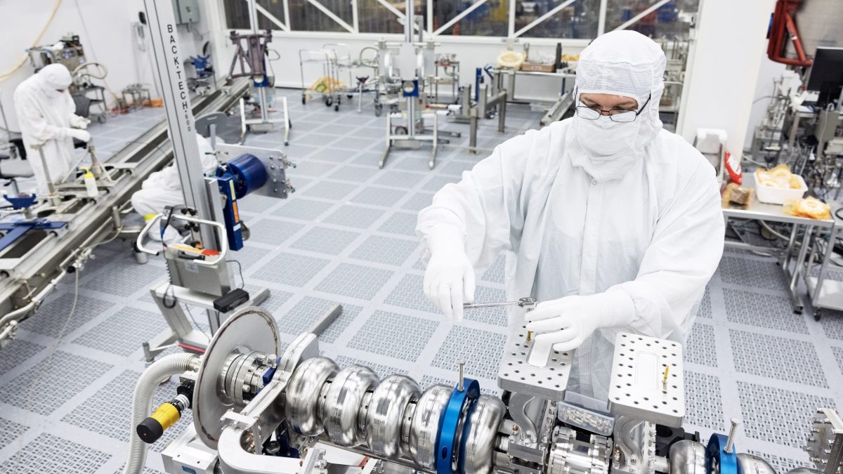
Featured image: A semiconductor clean room (file photo; a stand-in image, not the Sanand plant). Photo by Aileen Devlin/Jefferson Lab from Newport News, USA, in the public domain, via Wikimedia Commons.




Leave a Reply