



Headlines about India’s first “chip factory” can be confusing, because the word covers two very different kinds of plant. One kind makes the chips on silicon wafers and is called a fab. The other kind takes finished wafers and turns them into packaged, tested chips ready for use in a device, and is called an assembly, test, marking and packaging plant, or ATMP. Micron’s Sanand facility in Gujarat is the second kind, and the Tata-PSMC plant at Dholera is meant to be the first kind.
A fab is the front end of chipmaking. Circuit patterns are printed in many layers onto a silicon wafer in cleanrooms using extremely precise equipment, and the process determines how small and fast the chip can be. The Dholera plant is described as being designed for mature nodes of 28 to 110 nanometres, with a capacity of 50,000 wafers a month, and as costing about Rs 91,000 crore. Trial production is targeted for December 2026, according to reports.
An ATMP plant is the back end. It takes wafers that were made in a fab, cuts them into individual chips, packages them in protective casings, and tests them. Cleanroom Technology describes the Micron plant as converting DRAM and NAND wafers into finished memory and storage products, with a first-phase cleanroom of more than 500,000 square feet and Dell Technologies as the first customer.
The difference is in where the value lies. In a finished memory chip, most of the value and the hardest engineering are in the wafer made at the fab, so a plant that only packages and tests it adds a smaller part of the final value. The sources reviewed do not give percentages for this, and the split varies by product, so none is claimed here.
Why start with the back end? It is cheaper and quicker to build, it needs fewer specialised tools than a fab and it creates skilled jobs and customers, which helps the later fab projects. The India Semiconductor Mission has approved both types, with an overview in October 2026 listing 12 manufacturing units with combined investment of more than Rs 1.64 lakh crore, while another guide says 13 projects have been approved, so the count differs by source.
The mission supports projects through fiscal support covering up to 50% of the cost, according to the overview. That level of support is meant to offset the large costs and the risks of an industry that is dominated by a few countries. The sources reviewed do not describe whether the same share applies to every project.
There is also a third category, chip design. Companies that design chips without making them depend on fabs elsewhere, as the start-up Netrasemi does with its AI chip made at TSMC, according to a report on the company. The mission is trying to add manufacturing, packaging and testing around design.
What should readers watch? The first sign for the fab will be the trial run at Dholera, and for the assembly plants it will be the ramp of volumes from tens of millions of chips in 2026 to hundreds of millions in 2027, as projected for the Micron plant. Each step is a small part of a chain that takes years to build.
So when a headline says that India has opened a chip plant, the questions to ask are which stage of the process it covers and how much of the value is added in India, and in Sanand’s case it is the final stage of assembly and testing.
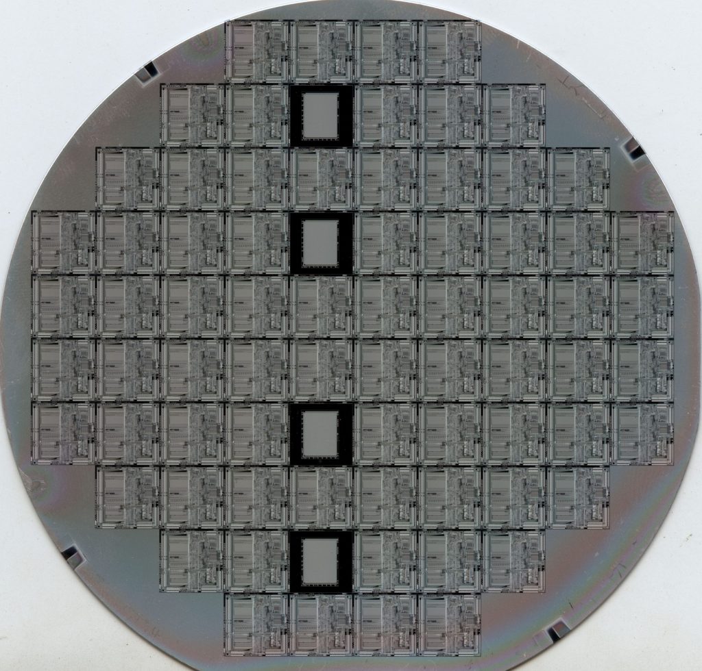
Featured image: A silicon wafer (file photo; a stand-in image). Photo by Retro-Computing Society of Rhode Island, licensed under CC BY-SA 4.0, via Wikimedia Commons.